2024 Year of the Summit Kicks Off – Meet us at MemCon

2023 was a great year for SNIA CMSI to meet with IT professionals and end users in “Summits” to discuss technologies, innovations, challenges, and solutions.  Our outreach at six industry events reached over 16,000 and we thank all who engaged with our CMSI members.

We are excited to continue a second “Year of the Summit” with a variety of opportunities to network and converse with you.  Our first networking event will take place March 26-27, 2024 at MemCon in Mountain View, CA.

MemCon 2024 focuses on systems design for the data centric era, working with data-intensive workloads, integrating emerging technologies, and overcoming data movement and management challenges. The agenda includes presentations and panels, featuring speakers from Meta, Microsoft, Netflix, Samsung, and Warner Brothers.   It’s the perfect event to discuss the integration of SNIA’s focus on developing global standards and delivering education on all technologies related to data.  SNIA and MemCon have prepared a video highlighting several of the key topics to be discussed.

MemCon 2024 Video Preview

At MemCon, SNIA CMSI member and SDXI Technical Work Group Chair Shyam Iyer of Dell will moderate a panel discussion on How are Memory Innovations Impacting the Total Cost of Ownership in Scaling-Up and Power Consumption , discussing impacts on hyperscalers, AI/ML compute, and cost/power.

SNIA Board member David McIntyre will participate in a panel on How are Increased Adoption of CXL, HBM, and Memory Protocol Expected to Change the Way Memory and Storage is Used and Assembled? , with insights on the markets and emerging memory innovations. The full MemCon agenda is here.

In the exhibit area, SNIA leaders will be on hand to demonstrate updates to the SNIA Persistent Memory Programming Workshop featuring new CXL® memory modules (get an early look at our Programming exercises here) and to provide a first look at a Smart Data Accelerator Interface (SDXI) specification implementation.  We’ll also provide updates on SNIA technical work on form factors like those used for CXL. We will feature a drawing for gift cards at the SNIA hosted coffee receptions and at the Tuesday evening networking reception.

SNIA colleagues and friends can register for MemCon with a 15% discount using code SNIA15.

And stay tuned for engaging with SNIA at upcoming events in 2024, including a return of the SNIA Compute, Memory, and Storage Summit in May 2024, August 2024 FMS-the Future of Memory and Storage; SNIA SDC in September, and SC24 in Atlanta in November 2024. We’ll discuss each of these in depth in our Year of the Summit blog series.

Emerging Memories Branch Out – a Q&A

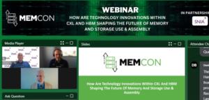
Our recent SNIA Persistent Memory SIG webinar explored in depth the latest developments and futures of emerging memories – now found in multiple applications both as stand-alone chips and embedded into systems on chips. We got some great questions from our live audience, and our experts Arthur Sainio, Tom Coughlin, and Jim Handy have taken the time to answer them in depth in this blog. And if you missed the original live talk, watch the video and download the PDF here.

Q:  Do you expect Persistent Memory to eventually gain the speeds that exist today with DRAM?

A:  It appears that that has already happened with the hafnium ferroelectrics that SK Hynix and Micron have shown.  Ferroelectric memory is a very fast technology and with very fast write cycles there should be every reason for it to go that way. With the hooks that are in CXL™, , though, that shouldn’t be that much of a problem since it’s a transactional protocol. The reads, then, will probably rival DRAM speeds for MRAM and for resistive RAM (MRAM might get up to DRAM speeds with its writes too). In fact, there are technologies like spin-orbit torque and even voltage-controlled magnetic anisotropy that promise higher performance and also low write latency for MRAM technologies. I think that probably most applications are read intensive and so the read is the real place where the focus is, but it does look like we are going to get there.

Q:  Are all the new Memory technology protocols (electrically) compatible to DRAM interfaces like DDR4 or DDR5? If not, then shouldn’t those technologies have lower chances of adoption as they add dependency on custom in-memory controller?

A:  That’s just a logic problem.  There’s nothing innate about any memory technology that couples it tightly with any kind of a bus, and so because NOR Flash and SRAM are the easy targets so far, most emerging technologies have used a NOR flash or SRAM type interface.  However, in the future they could use DDR.  There’re some special twists because you don’t have to refresh emerging memory technologies. but you know in general they could use DDR.

But one of the beauties of CXL is that you put anything you want to with any kind of interface on the other side of CXL and CXL erases what the differences are. It moderates them so although they may have different performances it’s hidden behind the CXL network.  Then the burden goes on to the CXL controller designers to make sure that those emerging technologies, whether it’s MRAM or others, can be adopted behind that CXL protocol. My expectation is for there to be a few companies early on who provide CXL controllers that that do have some kind of a specialty interface on them whether it’s for MRAM or for Resistive RAM or something like that, and then eventually for them to move their way into the mainstream.  Another interesting thing about CXL is that we may even see a hierarchy of different memories within CXL itself which also includes as part of CXL including domain specific processors or accelerators that operate close to memory, and so there are very interesting opportunities there as well. If you can do processing close to memory you lower the amount of data you’re moving around and you’re saving a lot of power for the computing system.

Q: Emerging memory technologies have a byte-level direct access programming model, which is in contrast to block-based NAND Flash. Do you think this new programming model will eventually replace NAND Flash as it reduces the overhead and reduces the power of transferring Data?

A: It’s a question of cost and that’s something that was discussed very much in our webinar. If you haven’t got a cost that’s comparable to NAND Flash, then you can’t really displace it.  But as far as the interface is concerned, the NAND interface is incredibly clumsy. All of these technologies do have both byte interfaces rather than a block interface but also, they can write in place – they don’t need to have a pre-erased block to write into. That from a technical standpoint is a huge advantage and now it’s just a question of whether or not they can get the cost down – which means getting the volume up.

Q: Can you discuss the High Bandwidth Memory (HBM) trends? What about memories used with Graphic Processing Units (GPUs)?

A: That topic isn’t the subject of this webinar as this webinar is about emerging memory technologies. But, to comment, we don’t expect to see emerging memory technologies adopt an HBM interface anytime in the really near future because HBM does springboard off DRAM and, as we discussed on one of the slides, DRAM has a transition that we don’t know when it’s going to happen that it goes to another emerging memory technology.  We’ve put it into the early 2030s in our chart, but it could be much later than that and HBM won’t convert over to an emerging memory technology until long after that.

However, HBM involves stacking of chips and that ultimately could happen.  It’s a more expensive process right now –  a way of getting a lot of memory very close to a processor – and if you look at some of the NVIDIA applications for example,  this is an example of the Chiplet technology and HBM can play a role in those Chiplet technologies for GPUs..  That’s another area that’s going to be using emerging memories as well – in the Chiplets.  While we didn’t talk about that so much in this webinar, it is another place for emerging memories to be playing a role.

There’s one other advantage to using an emerging memory that we did not talk about: emerging memories don’t need refresh. As a matter of fact, none of the emerging memory technologies need refresh. More power is consumed by DRAM refreshing than by actual data accesses.  And so, if you can cut that out of it,  you might be able to stack more chips on top of each other and get even more performance, but we still wouldn’t see that as a reason for DRAM to be displaced early on in HBM and then later on in the mainstream DRAM market.  Although, if you’re doing all those refreshes there’s a fair amount of potential of heat generation by doing that, which may have packaging implications as well. So, there may be some niche areas in there which could be some of the first ways in which some of these emerging memories are potentially used for those kinds of applications, if the performance is good enough.

Q:  Why have some memory companies failed?  Apart from the cost/speed considerations you mention, what are the other minimum envelope features that a new emerging memory should have? Is capacity (I heard 32Gbit multiple times) one of those criteria?

A: Shipping a product is probably the single most important activity for success. Companies don’t have to make a discrete or standalone SRAM or emerging memory chip but what they need to do is have their technology be adopted by somebody who is shipping something if they’re not going to ship it themselves.  That’s what we see in the embedded market as a good path for emerging memory IP: To get used and to build up volume. And as the volume and comfort with manufacturing those memories increase, it opens up the possibility down the road of lower costs with higher volume standalone memory as well.

Q:  What are the trends in DRAM interfaces?  Would you discuss CXL’s role in enabling composable systems with DRAM pooling?

A:  CXL, especially CXL 3.0, has particularly pointed at pooling. Pooling is going to be an extremely important development in memory with CXL, and it’s one of the reasons why CXL probably will proliferate. It allows you to be able to allocate memory which is not attached to particular server CPUs and therefore to make more efficient and effective use of those memories. We mentioned this earlier when we said that right now DRAM is that memory with some NAND Flash products out there too. But this could expand into other memory technologies behind CXL within the CXL pool as well as accelerators (domain specific processors) that do some operations closer to where the memory lives. So, we think there’s a lot of possibilities in that pooling for the development and growth of emerging memories as well as conventional memories.

Q: Do you think molecular-based technologies (DNA or others) can emerge in the coming years as an alternative to some of the semiconductor-based memories?

A: DNA and other memory technologies are in a relatively early stage but there are people who are making fairly aggressive plans on what they can do with those technologies. We think the initial market for those molecular memories are not in this high performance memory application; but especially with DNA, the potential density of storage and the fact that you can make lots of copies of content by using genetic genomic processes makes them very attractive potentially for archiving applications.  The things we’ve seen are mostly in those areas because of the performance characteristics. But the potential density that they’re looking at is actually aimed at that lower part of the market, so it has to be very, very cost effective to be able to do that, but the possibilities are there.  But again, as with the emerging high performance memories, you still have the economies of scale you have to deal with – if you can’t scale it fast enough the cost won’t go down enough that will actually will be able to compete in those areas. So it faces somewhat similar challenges, though in a different part of the market.

Earlier in the webcast, we said when showing the orb chart, that for something to fit into the computing storage hierarchy it has to be cheaper than the next faster technology and faster than the next cheaper technology. DNA is not a very fast technology and so that automatically says it has to be really cheap for it to catch on and that puts it in a very different realm than the emerging memories that we’re talking about here. On the other hand, you never know what someone’s going to discover, but right now the industry doesn’t know how to make fast molecular memories.

Q:  What is your intuition on how tomorrow’s highly dense memories might impact non-load/store processing elements such as AI accelerators? As model sizes continue to grow and energy density becomes more of an issue, it would seem like emerging memories could thrive in this type of environment. Your thoughts?

A:  Any memory would thrive in an environment where there was an unbridled thirst for memory. as artificial intelligence (AI) currently is. But AI is undergoing some pretty rapid changes, not only in the number of the parameters that are examined, but also in the models that are being used for it. We recently read a paper that was written by Apple* where they actually found ways of winnowing down the data that was used for a large language model into something that would fit into an Apple MacBook Pro M2 and they were able to get good performance by doing that.  They really accelerated things by ignoring data that didn’t really make any difference. So, if you take that kind of an approach and say: “Okay.  If those guys keep working on that problem that way, and they take it to the extreme, then you might not need all that much memory after all.”  But still, if memory were free, I’m sure that there’d be a ton of it out there and that is just a question of whether or not these memories can get cheaper than DRAM so that they can look like they’re free compared to what things look like today.

There are three interesting elements of this:  First, CXL, in addition allowing mixing of memory types, again allows you to put in those domain specific processors as well close to the memory. Perhaps those can do some of the processing that’s part of the model, in which case it would lower the energy consumption. The other thing it supports is different computing models than what we traditionally use. Of course there is quantum computing, but there also is something called neural networks which actually use the memory as a matrix multiplier, and those are using these emerging memories for that technology which could be used for AI applications.  The other thing that’s sort of hidden behind this is that spin tunnelling is changing processing itself in that right now everything is current-based, but there’s work going on in spintronic based devices that instead of using current would use the spin of electrons for moving data around, in which case we can avoid resistive heating and our processing could run a lot cooler and use less energy to do so.  So, there’s a lot of interesting things that are kind of buried in the different technologies being used for these emerging memories that actually could have even greater implications on the development of computing beyond just the memory application themselves.  And to elaborate on spintronics, we’re talking about logic and not about spin memory – using spins rather than that of charge which is current.

Q:  Flash has an endurance issue (maximum number of writes before it fails). In your opinion, what is the minimum acceptable endurance (number of writes) that an emerging memory should support?

It’s amazing how many techniques have fallen into place since wear was an issue in flash SSDs.  Today’s software understands which loads have high write levels and which don’t, and different SSDs can be used to handle the two different kinds of load.  On the SSD side, flash endurance has continually degraded with the adoption of MLC, TLC, and QLC, and is sometimes measured in the hundreds of cycles.  What this implies is that any emerging memory can get by with an equally low endurance as long as it’s put behind the right controller.

In high-speed environments this isn’t a solution, though, since controllers add latency, so “Near Memory” (the memory tied directly to the processor’s memory bus) will need to have higher endurance.  Still, an area that can help to accommodate that is the practice of putting code into memories that have low endurance and data into higher-endurance memory (which today would be DRAM).  Since emerging memories can provide more bits at a lower cost and power than DRAM, the write load to the code space should be lower, since pages will be swapped in and out more frequently.  The endurance requirements will depend on this swapping, and I would guess that the lowest-acceptable level would be in the tens of thousands of cycles.

Q: It seems that persistent memory is more of an enterprise benefit rather than a consumer benefit. And consumer acceptance helps the advancement and cost scaling issues. Do you agree? I use SSDs as an example. Once consumers started using them, the advancement and prices came down greatly.

Anything that drives increased volume will help.  In most cases any change to large-scale computing works its way down to the PC, so this should happen in time here, too. But today there’s a growing amount of MRAM use in personal fitness monitors, and this will help drive costs down, so initial demand will not exclusively come from enterprise computing. At the same time, the IBM FlashDrive that we mentioned uses MRAM, too, so both enterprise and consumer are already working to simultaneously grow consumption.

Q: The CXL diagram (slide 22 in the PDF) has 2 CXL switches between the CPUs and the memory. How much latency do you expect the switches to add, and how does that change where CXL fits on the array of memory choices from a performance standpoint?

The CXL delay goals are very aggressive, but I am not sure that an exact number has been specified.  It’s on the order of 70ns per “Hop,” which can be understood as the delay of going through a switch or a controller. Naturally, software will evolve to work with this, and will move data that has high bandwidth requirements but is less latency-sensitive to more remote areas, while managing the more latency-sensitive data to near memory.

Q: Where can I learn more about the topic of Emerging Memories?

Here are some resources to review


* LLM in a Flash: Efficient Large Language Model Inference with Limited Memory, Kevin Avizalideh, et. al.,             arXiv:2312.11514 [cs.CL]

Open Standards Featured at FMS 2023

SNIA welcomes colleagues to join them at the upcoming Flash Memory Summit, August 8-10, 2023 in Santa Clara CA.

SNIA is pleased to join standards organizations CXL Consortium™ (CXL™), PCI-SIG®, and Universal Chiplet Interconnect Express™ (UCIe™) in an Open Standards Pavilion, Booth #725, in the Exhibit Hall.  CMSI will feature SNIA member companies in a computational storage cross industry demo by Intel, MINIO, and Solidigm and a Data Filtering demo by ScaleFlux; a software memory tiering demo by VMware; a persistent memory workshop and hackathon; and the latest on SSD form factors E1 and E3 work by SNIA SFF TA Technical work group. SMI will showcase SNIA Swordfish® management of NVMe SSDs on Linux with demos by Intel Samsung and Solidigm.

CXL will discuss their advances in coherent connectivity.  PCI-SIG will feature their PCIe 5.0 architecture (32GT/s) and PCIe 6.0 (65GT/s) architectures and industry adoption and the upcoming PCIe 7.0 specification development (128GT/s).  UCIe will discuss their new open industry standard establishing a universal interconnect at the package-level.

SNIA STA Forum will also be in Booth #849 – learn more about the SCSI Trade Association joining SNIA.

These demonstrations and discussions will augment FMS program sessions in the SNIA-sponsored System Architecture Track on memory, computational storage, CXL, and UCIe standards.  A SNIA mainstage session on Wednesday August 9 at 2:10 pm will discuss Trends in Storage and Data: New Directions for Industry Standards.

SNIA colleagues and friends can receive a $100 discount off the 1-, 2-, or 3-day full conference registration by using code SNIA23.

Visit snia.org/fms to learn more about the exciting activities at FMS 2023 and join us there!

Your Questions Answered on Persistent Memory, CXL, and Memory Tiering

With the persistent memory ecosystem continuing to evolve with new interconnects like CXL™ and applications like memory tiering, our recent Persistent Memory, CXL, and Memory Tiering-Past, Present, and Future webinar was a big success.  If you missed it, watch it on demand HERE!

Many questions were answered live during the webinar, but we did not get to all of them.  Our moderator Jim Handy from Objective Analysis, and experts Andy Rudoff and Bhushan Chithur from Intel, David McIntyre from Samsung, and Sudhir Balasubramanian and Arvind Jagannath from VMware have taken the time to answer them in this blog. Happy reading!

Q: What features or support is required from a CXL capable endpoint to e.g. an accelerator to support the memory pooling? Any references?

A: You will have two interfaces, one for the primary memory accesses and one for the management of the pooling device. The primary memory interface is the .mem and the management interface will be via the .io or via a sideband interface. In addition you will need to implement a robust failure recovery mechanism since the blast radius is much larger with memory pooling.

Q: How do you recognize weak information security (in CXL)?

A: CXL has multiple features around security and there is considerable activity around this in the Consortium.  For specifics, please see the CXL Specification or send us a more specific question.

Q: If the system (e.g. x86 host) wants to deploy CXL memory (Type 3) now, is there any OS kernel configuration, BIO configuration to make the hardware run with VMWare (ESXi)? How easy or difficult this setup process?

A: A simple CXL Type 3 Memory Device providing volatile memory is typically configured by the pre-boot environment and reported to the OS along with any other main memory.  In this way, a platform that supports CXL Type 3 Memory can use it without any additional setup and can run an OS that contains no CXL support and the memory will appear as memory belonging to another NUMA code.  That said, using an OS that does support CXL enables more complex management, error handling, and more complex CXL devices.

Q: There was a question on ‘Hop” length. Would you clarify?

A: In the webinar around minute 48, it was stated that a Hop was 20ns, but this is not correct. A Hop is often spoken of as “Around 100ns.”  The Microsoft Azure Pond paper quantifies it four different ways, which range from 85ns to 280ns.

Q: Do we have any idea how much longer the latency will be?  

A: The language CXL folks use is “Hops.”   An address going into CXL is one Hop, and data coming back is another.  In a fabric it would be twice that, or four Hops.  The  latency for a Hop is somewhere around 100ns, although other latencies are accepted.

Q: For memory semantic SSD:  There appears to be a trend among 2LM device vendors to presume the host system will be capable of providing telemetry data for a device-side tiering mechanism to decide what data should be promoted and demoted.  Meanwhile, software vendors seem to be focused on the devices providing telemetry for a host-side tiering mechanism to tell the device where to move the memory.  What is your opinion on how and where tiering should be enforced for 2LM devices like a memory semantic SSD?

A: Tiering can be managed both by the host and within computational storage drives that could have an integrated compute function to manage local tiering- think edge applications.

Q: Re VM performance in Tiering: It appears you’re comparing the performance of 2 VM’s against 1.  It looked like the performance of each individual VM on the tiering system was slower than the DRAM only VM.  Can you explain why we should take the performance of 2 VMs against the 1 VM?  Is the proposal that we otherwise would have required those 2 VM’s to run on separate NUMA node, and now they’re running on the same NUMA node?

A: Here the use case was, lower TCO & increased capacity of memory along with aggregate performance of VM’s v/s running few VM’s on DRAM. In this use case, the DRAM per NUMA Node was 384GB, the Tier2 memory per NUMA node was 768GB. The VM RAM was 256GB.

In the DRAM only case, if we have to run business critical workloads e.g., Oracle with VM RAM=256GB,  we could only run 1 VM (256GB) per NUMA Node (DRAM=384GB), we cannot over-provision memory in the DRAM only case as every NUMA node has 384GB only. So potentially we could run 4 such VM’s (VM RAM=256Gb) in this case with NUMA node affinity set as we did in this use case OR if we don’t do NUMA node affinity, maybe 5 such VM’s without completely maxing out the server RAM.  Remember, we did NUMA node affinity in this use case to eliminate any cross NUMA latency.78

Now with Tier2 memory in the mix, each NUMA node has 384GB DRAM and 768GB Tier2 Memory, so theoretically one could run 16-17 such VM’s (VM RAM =256GB), hence we are able to increase resource maximization, run more workloads, increase transactions etc , so lower TCO, increased capacity and aggregate performance improvement.

Q: CXL is changing very fast, we have 3 protocol versions in 2 years, as a new consumer of CXL what are the top 3 advantages of adopting CXL right away v/s waiting for couple of more years?

A: All versions of CXL are backward compatible.  Users should have no problem using today’s CXL devices with newer versions of CXL, although they won’t be able to take advantage of any new features that are introduced after the hardware is deployed.

Q: (What is the) ideal when using agilex FPGAs as accelerators?

A: CXL 3.0 supports multiple accelerators via the CXL switching fabric. This is good for memory sharing across heterogeneous compute accelerators, including FPGAs.

Thanks again for your support of SNIA education, and we invite you to write askcmsi@snia.org for your ideas for future webinars and blogs!

It’s A Wrap – But Networking and Education Continue From Our C+M+S Summit!

Our 2023 SNIA Compute+Memory+Storage Summit was a success! The event featured 50 speakers in 40 sessions over two days. Over 25 SNIA member companies and alliance partners participated in creating content on computational storage, CXL™ memory, storage, security, and UCIe™. All presentations and videos are free to view at www.snia.org/cms-summit.

“For 2023, the Summit scope expanded to examine how the latest advances within and across compute, memory and storage technologies should be optimized and configured to meet the requirements of end customer applications and the developers that create them,” said David McIntyre, Co-Chair of the Summit.  “We invited our SNIA Alliance Partners Compute Express Link™ and Universal Chiplet Interconnect Express™ to contribute to a holistic view of application requirements and the infrastructure resources that are required to support them,” McIntyre continued.  “Their panel on the CXL device ecosystem and usage models and presentation on UCIe innovations at the package level along with three other sessions on CXL added great value to the event.”

Thirteen computational storage presentations covered what is happening in NVMe™ and SNIA to support computational storage devices and define new interfaces with computational storage APIs that work across different hardware architectures.  New applications for high performance data analytics, discussions of how to integrate computational storage into high performance computing designs, and new approaches to integrate compute, data and I/O acceleration closely with storage systems and data nodes were only a few of the topics covered.

“The rules by which the memory game is played are changing rapidly and we received great feedback on our nine presentations in this area,” said Willie Nelson, Co-Chair of the Summit.  “SNIA colleagues Jim Handy and Tom Coughlin always bring surprising conclusions and opportunities for SNIA members to keep abreast of new memory technologies, and their outlook was complimented by updates on SNIA standards on memory-to memory data movement and on JEDEC memory standards; presentations on thinking memory, fabric attached memory, and optimizing memory systems using simulations; a panel examining where the industry is going with persistent memory, and much more.”

Additional highlights included an EDSFF panel covering the latest SNIA specifications that support these form factors, sharing an overview of platforms that are EDSFF-enabled, and discussing the future for new product and application introductions; a discussion on NVMe as a cloud interface; and a computational storage detecting ransomware session.

New to the 2023 Summit – and continuing to get great views – was a “mini track” on Security, led by Eric Hibbard, chair of the SNIA Storage Security Technical Work Group with contributions from IEEE Security Work Group members, including presentations on cybersecurity, fine grain encryption, storage sanitization, and zero trust architecture.

Co-Chairs McIntyre and Nelson encourage everyone to check out the video playlist and send your feedback to askcmsi@snia.org. The “Year of the Summit” continues with networking opportunities at the upcoming SmartNIC Summit (June), Flash Memory Summit (August), and SNIA Storage Developer Conference (September).  Details on all these events and more are at the SNIA Event Calendar page.  See you soon!

50 Speakers Featured at the 2023 SNIA Compute+Memory+Storage Summit

SNIA’s Compute+Memory+Storage Summit is where architectures, solutions, and community come together. Our 2023 Summit – taking place virtually on April 11-12, 2023 – is the best example to date, featuring a stellar lineup of 50 speakers in 40 sessions covering topics including computational storage real-world applications, the future of memory, critical storage security issues, and the latest on SSD form factors, CXL™, and UCIe™.

“We’re excited to welcome executives, architects, developers, implementers, and users to our 11th annual Summit,” said David McIntyre, C+M+S Summit Co-Chair, and member of the SNIA Board of Directors.  “We’ve gathered the technology leaders to bring us the latest developments in compute, memory, storage, and security in our free online event.  We hope you will watch live to ask questions of our experts as they present, and check out those sessions you miss on-demand.”

Memory sessions begin with Watch Out – Memory’s Changing! where Jim Handy and Tom Coughlin will discuss the memory technologies vying for the designer’s attention, with CXL™ and UCIe™ poised to completely change the rules. Speakers will also cover thinking memory, optimizing memory using simulations, providing capacity and TCO to applications using software memory tiering, and fabric attached memory.

Compute sessions include Steven Yuan of StorageX discussing the Efficiency of Data Centric Computing, and presentations on the computational storage and compute market, big-disk computational storage arrays for data analytics, NVMe as a cloud interface, improving storage systems for simulation science with computational storage, and updates on SNIA and NVM Express work on computational storage standards.

CXL and UCIe will be featured with presentations on CXL 3.0 and Universal Compute Interface Express™ On-Package Innovation Slot for Compute, Memory, and Storage Applications.

The Summit will also dive into security with a introductory view of today’s storage security landscape and additional sessions on zero trust architecture, storage sanitization, encryption, and cyber recovery and resilience.

For 2023, the Summit is delighted to present three panels – one on Exploring the Compute Express Link™ (CXL™) Device Ecosystem and Usage Models moderated by Kurtis Bowman of the CXL Consortium, one on Persistent Memory Trends moderated by Dave Eggleston of Microchip, and one on Form Factor Updates, moderated by Cameron Brett of the SNIA SSD Special Interest Group.

We will also feature the popular SNIA Birds-of-a-Feather sessions. On Tuesday April 11 at 4:00 pm PDT/7:00 pm EDT, you can join to discuss the latest compute, memory, and storage developments, and on Wednesday April at 3:00 pm PDT/6:00 pm EDT, we’ll be talking about memory advances.

Learn more in our Summit preview video, check out the agenda, and register for free to access our Summit platform!

“Year of the Summit” Kicks Off with Live and Virtual Events

For 11 years, SNIA Compute, Memory and Storage Initiative (CMSI) has presented a Summit featuring industry leaders speaking on the key topics of the day.  In the early years, it was persistent memory-focused, educating audiences on the benefits and uses of persistent memory.  In 2020 it expanded to a Persistent Memory+Computational Storage Summit, examining that new technology, its architecture, and use cases.

Now in 2023, the Summit is expanding again to focus on compute, memory, and storage.  In fact, we’re calling 2023 the Year of the Summit – a year to get back to meeting in person and offering a variety of ways to listen to leaders, learn about technology, and network to discuss innovations, challenges, solutions, and futures.

We’re delighted that our first event of the Year of the Summit is a networking event at MemCon, taking place March 28-29 at the Computer History Museum in Mountain View CA.

At MemCon, SNIA CMSI member and IEEE President elect Tom Coughlin of Coughlin Associates will moderate a panel discussion on Compute, Memory, and Storage Technology Trends for the Application Developer.  Panel members Debendra Das Sharma of Intel and the CXL™ Consortium, David McIntyre of Samsung and the SNIA Board of Directors, Arthur Sainio of SMART Modular and the SNIA Persistent Memory Special Interest Group, and Arvind Jaganath of VMware and SNIA CMSI will examine how applications and solutions available today offer ways to address enterprise and cloud provider challenges – and they’ll provide a look to the future.

SNIA leaders will be on hand to discuss work in computational storage, smart data acceleration interface (SDXI), SSD form factor advances, and persistent memory trends.  Share a libation or two at the SNIA hosted networking reception on Tuesday evening, March 28.

This inaugural MemCon event is perfect to start the conversation, as it focuses on the intersection between systems design, memory innovation (emerging memories, storage & CXL) and other enabling technologies. SNIA colleagues and friends can register for MemCon with a 15% discount using code SNIA15.

April 2023 Networking!

We will continue the Year with a newly expanded SNIA Compute+Memory+Storage Summit coming up April 11-12 as a virtual event.  Complimentary registration is now open for a stellar lineup of speakers, including Stephen Bates of Huawei, Debendra Das Sharma of  Universal Chiplet Interconnect Express™, Jim Handy of Objective Analysis, Shyam Iyer of Dell, Bill Martin of Samsung, Jake Oshins of Microsoft, Andy Rudoff of Intel, Andy Walls of IBM, and Steven Yuan of StorageX.

Summit topics include Memory’s Headed for Change, High Performance Data Analytics, CXL 3.0, Detecting Ransomware, Meeting Scaling Challenges, Open Standards for Innovation at the Package Level, and Standardizing Memory to Memory Data Movement. Great panel discussions are on tap as well.  Kurt Lender of the CXL Consortium will lead a discussion on Exploring the CXL Device Ecosystem and Usage Models, Dave Eggleston of Microchip will lead a panel with Samsung and SMART Modular on Persistent Memory Trends, and Cameron Brett of KIOXIA will lead a SSD Form Factors Update.   More details at www.snia.org/cms-summit.

Later in 2023…

Opportunities for networking will continue throughout 2023. We look forward to seeing you at the SmartNIC Summit (June 13-15), Flash Memory Summit (August 8-10), SNIA Storage Developer Conference (September 18-21), OCP Global Summit (October 17-19), and SC23 (November 12-17). Details on SNIA participation coming soon!

Join Us as We Return Live to FMS!

SNIA is pleased to be part of the Flash Memory Summit 2022 agenda August 1-4, 2022 at the Santa Clara CA Convention Center, with our volunteer leadership demonstrating solutions, chairing and speaking in sessions, and networking with FMS attendees at a variety of venues during the conference.

The ever-popular SNIA Reception at FMS features the SNIA groups Storage Management Initiative, Compute Memory and Storage Initiative, and Green Storage Initiative, along with SNIA alliance partners CXL Consortium, NVM Express, and OpenFabrics Alliance.  Stop by B-203/204 at the Convention Center from 5:30 – 7:00 pm Monday August 1 for refreshments and networking with colleagues to kick off the week!

You won’t want to miss SNIA’s mainstage presentation on Wednesday August 3 at 2:40 pm in the Mission City Ballroom. SNIA Vice Chair Richelle Ahlvers of Intel will provide a perspective on how new storage technologies and trends are accelerating through standards and open communities.

In the Exhibit Hall, SNIA Storage Management Initiative and Compute Memory and Storage Initiative are FMS Platinum sponsors with a SNIA Demonstration Pavilion at booth #725.  During exhibit hours Tuesday evening through Thursday afternoon, 15 SNIA member companies will be featured in live technology demonstrations on storage management, computational storage, persistent memory, sustainability, and form factors; a Persistent Memory Programming Workshop and Hackathon; and theater presentations on SNIA’s standards and alliance work. 

Long standing SNIA technology focus areas in computational storage and memory will be represented in the SNIA sponsored System Architectures Track (SARC for short) – Tuesday for memory and Thursday for computational storage.  SNIA is also pleased to sponsor a day on CXL architectures, memory, and storage talks on Wednesday. These sessions will all be in Ballroom G.

A new Sustainability Track on Thursday morning in Ballroom A led by the SNIA Green Storage Technical Work Group includes presentations on SSD power management, real world applications and storage workloads, and a carbon footprint comparison of SSDs vis HDDs, followed by a panel discussion. SSDs will also be featured in two SNIA-led presentation/panel pairs – SSDS-102-1 and 102-2 Ethernet SSDs on Tuesday afternoon in Ballroom B and SSDS-201-1 and 201-2 EDSFF E1 and E3 form factors on Wednesday morning in Ballroom D. SNIA Swordfish will be discussed in the DCTR-102-2 Enterprise Storage Part 2 session in Ballroom D on Tuesday morning

And the newest SNIA technical work group – DNA Data Storage– will lead a new-to-2022 FMS track on Thursday morning in Great America Meeting Room 2, discussing topics like preservation of DNA for information storage, the looming need for molecular storage, and DNA sequencing at scale. Attendees can engage for questions and discussion in Part 2 of the track.

Additional ways to network with SNIA colleagues include the always popular chat with the experts – beer and pizza on Tuesday evening, sessions on cloud storage, artificial intelligence, blockchain, and an FMS theater presentation on real world storage workloads.

Full details on session times, locations, chairs and speakers for all these exciting FMS activities can be found at www.snia.org/fms and on the Flash Memory Summit website.  SNIA colleagues and friends can register for $100.00 off the full conference or single day packages using the code SNIA22 at www.flashmemorysummit.com.

Summit Success – and A Preview of What’s To Come

Last month’s SNIA Persistent Memory and Computational Storage Summit (PM+CS Summit) put on a great show with 35 technology presentations from 41 speakers. Every presentation is now available online with a video and PDF found at www.snia.org/pm-summit.

Recently, SNIA On Storage sat down with David McIntyre, Summit Chair from Samsung, on his impressions of this 10th annual event.

SNIA On Storage (SOS): What were your thoughts on key topics coming into the Summit and did they change based on the presentations?

David McIntyre (DM): We were excited to attract technology leaders to speak on the state of computational storage and persistent memory.  Both mainstage and breakout speakers did a good job of encapsulating and summarizing what is happening today.  Through the different talks, we learned more about infrastructure deployments supporting underlying applications and use cases. A new area where attendees gained insight was computational memory. 

I find it encouraging that as an industry we are moving forward on focusing on applications and use cases, and supporting software and infrastructure that resides across persistent memory and computational storage.  And with computational memory, we are now getting more into the system infrastructure concerns and making these technologies more accessible to application developers.

SOS: Any sessions you want to recommend to viewers?

DM: We had great feedback on our speakers during the live event.  Several sessions I might recommend are Gary Grider of Los Alamos National Labs (LANL), who explained how computational storage is being deployed across his lab; Chris Petersen of Meta, who took an infrastructure view on considerations for persistent memory and computational storage; and Andy Walls of IBM, who presented a nice viewpoint of his vision of computational storage and its underlying benefits that make the overall infrastructure more rich and efficient, and how to bring compute to the drives.  For a summary, watch Dave Eggleston of In-Cog Computing who led Tuesday and Wednesday panels with the mainstage speakers that provided a wide ranging discussion on the Summit’s key topics.

SOS: What do you see as the top takeaways from the Summit presenters?

DM: I see three:

  1. Infrastructure, applications, and use cases were paramount themes across a number of presentations
  2. Tighter coupling of technologies.  Cheolmin Park of Samsung, in his CXL and UCIe presentation, discussed how we already have point technologies that now need to interact together.  There is also the Persistent Memory/SSD/DRAM combination – a tiered memory configuration talked about for years.  We are seeing deployment use cases where the glue is interfacing the I/O technology with CXL and UCIe.
  3. Another takeaway strongly related to the above is heterogeneous operations and compute.  Compute can’t reside in one central location for efficiency.  Rather, it must be distributed – addressing real-time analytics and decision making to support applications.

SOS: What upcoming activities should Summit viewers plan to attend and why?

DM: Put Flash Memory Summit, August 1-4, 2022 on your calendars.  Here SNIA will go deeper into areas we explored at the Summit.

First, join SNIA Compute, Memory, and Storage Initiative (CMSI), underwriter of the PM+CS Summit, as we meet in person for the first time in a long time at the SNIA Reception on Monday evening August 1 at the Santa Clara Convention Center from 5:30 pm – 7:00 pm. Along with our SNIA teammates from the SNIA Storage Management Initiative, network with colleagues and share an appetizer or two as we gear up for three full days of activities. 

At the Summit, the SNIA-sponsored System Architectures Track will feature a day on persistent memory, a day on CXL, and a day on computational storage.  SNIA will also lead sessions on form factors, ethernet SSDs, sustainability, and DNA data storage.  I am Track Manager of the Artificial Intelligence Applications Track, where we will see how technologies like computational storage and AI work hand-in-hand.

SNIA will have a Demonstration Pavilion at booth 725 in the FMS Exhibit Hall with live demonstrations of computational storage applications, persistent memory implementations, and scalable storage management with SNIA Alliance Partners; hands-on form factor displays; a Persistent Memory Programming Workshop and Hackathon; and theater presentations on standards. Full details are at www.flashmemorysummit.com

In September, CMSI will be at the SNIA Storage Developer Conference where we will celebrate SNIA’s 25th anniversary and gather in person for sessions, demonstrations, and those ever popular Birds-of-a-Feather sessions.  Find the latest details at www.storagedeveloper.org.

SOS: Any final thoughts?

DM: On behalf of SNIA CMSI and the PM+CS Summit Planning Team, I’d like to thank all those who planned and attended our great event.  We are progressing in the right direction, beginning to talk the same language that application developers and solution providers understand.  We’ll keep building our strategic collaboration across different worlds at FMS and SDC.  I appreciate the challenges and working together.

See You – Virtually – at SDC 2021

SNIA Storage Developer Conference goes virtual September 28-29 2021, and compute, memory, and storage are important topics.  SNIA Compute, Memory, and Storage Initiative is a sponsor of SDC 2021 – so visit our booth for the latest information and a chance to chat with our experts.  With over 120 sessions available to watch live during the event and later on-demand, live Birds of a Feather chats, and a Persistent Memory Bootcamp and Hackathon accessing new systems in the cloud, we want to make sure you don’t miss anything!  Register here to see sessions live – or on demand to your schedule. 

Agenda highlights include:

LIVE Birds of a Feather Sessions are OPEN to all – SDC registration not required. Here is your chance, via zoom, to ask your questions of the SNIA experts.  Registration links will go live on September 28 and 29 at this page link.

Computational Storage Talks

A great video provides an overview of sessions. Watch it here.

  • Computational Storage APIs – how the SNIA Computational Storage TWG is leading the way with new interface definitions with Computational Storage APIs that work across different hardware architectures.
  • NVMe Computational Storage Update – Learn what is happening in NVMe to support Computational Storage devices, including a high level architecture that is being defined in NVMe for Computational Storage. The architecture provides for programs based on a standardized eBPF. (Check out our blog on eBPF.)

Persistent Memory Presentations

A great video provides an overview of sessions. Watch it here.